


Introduction
Atomic Force Microscopy (AFM) is a high-resolution scanning probe microscopy technique used to measure and visualize surfaces at the nanometer and atomic scale. It is widely used in nanotechnology, materials science, biology, chemistry, and physics to study the structure and properties of surfaces.
AFM was invented in 1986 by Gerd Binnig, Calvin Quate, and Christoph Gerber. It was developed as an extension of the scanning tunneling microscope but with the advantage that it can image both conductive and non-conductive materials.
Unlike optical microscopes, AFM does not rely on light. Instead, it measures tiny forces between a sharp probe and the sample surface. These forces are extremely small—often on the order of piconewtons—and arise from interactions between atoms in the probe tip and atoms in the sample.
AFM can produce three-dimensional surface images with extremely high resolution, making it one of the most important tools for nanoscale research.
Basic Principle of Atomic Force Microscopy
The fundamental principle behind AFM is the measurement of interatomic forces between a sharp probe and the surface of a sample.
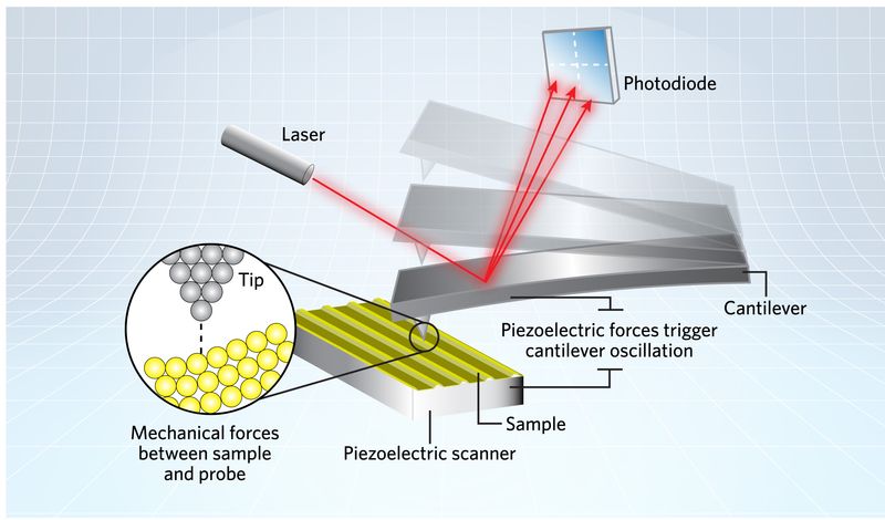
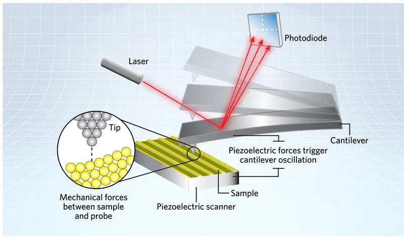
A tiny probe tip mounted on a flexible cantilever scans across the surface of the sample. As the tip interacts with atoms on the surface, forces cause the cantilever to bend or deflect.
These deflections are detected using a laser beam and photodetector system.
The interaction between the probe and the surface is often modeled using Hooke’s law, which relates force to displacement of the cantilever.
genui{“math_block_widget_common_keywords”:{“content”:”F = -kx”}}
where:
- (F) = force acting on the cantilever
- (k) = spring constant of the cantilever
- (x) = displacement of the cantilever
By measuring the cantilever deflection, the AFM can determine the forces acting on the tip and reconstruct a detailed surface image.
Main Components of an Atomic Force Microscope


An atomic force microscope consists of several key components that work together to produce nanoscale images.
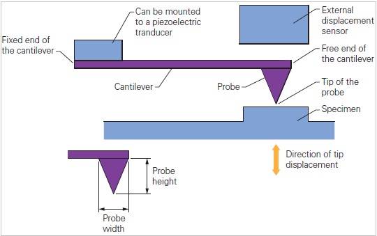
Cantilever and Probe Tip
The cantilever is a small flexible beam with a sharp probe tip at its end.
The tip radius may be only a few nanometers wide.
As the tip scans the surface, forces between the tip and sample cause the cantilever to bend.
Laser and Photodetector
A laser beam is reflected off the back of the cantilever onto a photodetector.
When the cantilever bends, the laser reflection changes position on the detector.
This allows extremely precise measurement of cantilever deflection.
Piezoelectric Scanner
Piezoelectric materials expand or contract when voltage is applied.
AFM uses piezoelectric scanners to move the sample or tip with atomic precision in the x, y, and z directions.
Feedback System
The feedback system maintains a constant interaction force between the tip and surface.
It adjusts the tip height as the surface changes during scanning.
Interatomic Forces in AFM
AFM works by measuring forces between atoms.
These forces include:
- Van der Waals forces
- Electrostatic forces
- Chemical bonding forces
- Magnetic forces
At very small distances, repulsive forces occur due to electron cloud interactions.
At slightly larger distances, attractive forces dominate.
These interactions allow AFM to detect surface features with extremely high sensitivity.
Operating Modes of AFM
AFM can operate in several different modes depending on how the probe interacts with the surface.
Contact Mode


In contact mode, the probe tip remains in direct contact with the surface.
The cantilever bends as the tip encounters surface features.
Advantages:
- High-resolution images
- Fast scanning
Limitations:
- Can damage delicate samples
- Friction between tip and surface
Non-Contact Mode


In non-contact mode, the cantilever oscillates near the surface without touching it.
The tip senses attractive forces between atoms.
Advantages:
- Minimal damage to samples
- Suitable for delicate materials
Tapping Mode (Intermittent Contact)

In tapping mode, the cantilever oscillates and periodically touches the surface.
This mode combines advantages of contact and non-contact modes.
Advantages:
- Reduced sample damage
- High-resolution imaging
Tapping mode is widely used for imaging soft materials.
AFM Image Formation
AFM images are created by scanning the probe across the surface in a raster pattern.
During scanning:
- The probe moves across the sample line by line.
- Cantilever deflections are measured.
- The feedback system adjusts the probe height.
- Data is recorded and converted into a 3D surface map.
The resulting images show surface topography with nanometer or atomic resolution.
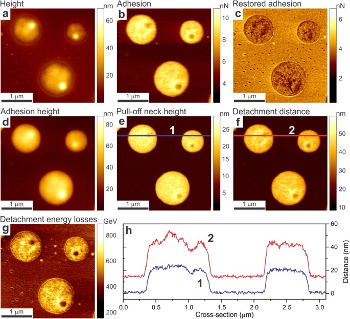
Types of AFM Measurements
AFM can measure more than just surface height.
Different measurement modes allow analysis of many material properties.
Examples include:
- Surface roughness
- Mechanical stiffness
- Adhesion forces
- Electrical conductivity
- Magnetic properties
AFM can also measure friction between surfaces.
Applications of Atomic Force Microscopy
AFM has numerous applications in science and engineering.
Nanotechnology
AFM is widely used for studying nanoscale materials.
Researchers examine nanoparticles, nanowires, and graphene surfaces.
Materials Science
AFM helps analyze:
- Surface roughness
- Thin films
- Crystal structures
- Surface defects
Biology
AFM can image biological structures such as:
- DNA molecules
- Proteins
- Cell membranes
- Viruses
Unlike electron microscopy, AFM can operate in liquid environments, allowing observation of biological samples in near-natural conditions.
Semiconductor Industry
AFM is used to inspect semiconductor surfaces and nanostructures.
This helps improve microchip fabrication processes.
Surface Chemistry
AFM can study chemical reactions occurring on surfaces at the nanoscale.
Advantages of AFM
AFM provides several advantages compared to other microscopy techniques.
Atomic Resolution
AFM can achieve atomic-level imaging.
Works with Non-Conductive Samples
Unlike scanning tunneling microscopy, AFM can image insulating materials.
Three-Dimensional Imaging
AFM produces true 3D surface maps.
Works in Air or Liquid
AFM can operate in various environments.
Limitations of AFM
Despite its advantages, AFM has some limitations.
Small Scan Area
AFM typically scans areas only a few micrometers wide.
Slow Scanning
High-resolution imaging can take significant time.
Tip Wear
The probe tip can become worn or damaged.
Complex Operation
AFM requires precise control and calibration.
Advanced AFM Techniques
Modern AFM systems incorporate many advanced capabilities.
Examples include:
- Magnetic force microscopy
- Electrostatic force microscopy
- Kelvin probe force microscopy
- Conductive AFM
These techniques allow measurement of electrical, magnetic, and mechanical properties at the nanoscale.
Future Developments in AFM
Advances in atomic force microscopy continue to expand its capabilities.
Future improvements may include:
- Faster scanning speeds
- Higher resolution imaging
- Improved probe materials
- Integration with other analytical techniques
AFM will remain an essential tool for nanoscale research and nanotechnology development.
Conclusion
Atomic force microscopy is one of the most important tools for studying surfaces at the nanometer and atomic scale. By measuring tiny forces between a probe tip and a sample surface, AFM can produce detailed three-dimensional images of materials.
Since its invention, AFM has transformed research in nanotechnology, materials science, biology, and semiconductor engineering. Its ability to image non-conductive materials and operate in various environments makes it more versatile than many other microscopy techniques.
With ongoing technological advancements, AFM continues to play a crucial role in exploring the nanoscale world and advancing scientific understanding of materials and biological systems.