


Introduction
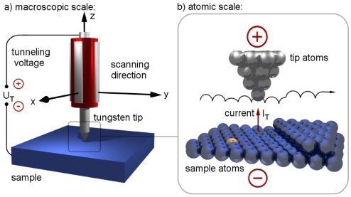
Scanning tunneling microscopy (STM) is a powerful surface imaging technique that allows scientists to visualize and manipulate individual atoms on the surface of materials. It is one of the most important tools in nanotechnology and surface science. STM provides images with atomic-scale resolution and enables researchers to study electronic properties of surfaces with extraordinary precision.
STM was invented in 1981 by Gerd Binnig and Heinrich Rohrer at IBM. Their invention revolutionized the field of microscopy and earned them the Nobel Prize in Physics in 1986.
Unlike optical microscopes or even electron microscopes, STM does not rely on light or electron beams to form images. Instead, it uses the principles of quantum tunneling, a phenomenon predicted by quantum mechanics.
By measuring the tunneling current between a sharp metal tip and a conducting surface, STM can map the atomic structure of materials with extremely high resolution.
STM has become essential for research in physics, chemistry, materials science, nanotechnology, and semiconductor engineering.
Basic Principle of Scanning Tunneling Microscopy
The operation of STM is based on the quantum tunneling effect.
According to classical physics, electrons cannot pass through a potential barrier if they do not possess enough energy. However, quantum mechanics allows electrons to penetrate through barriers under certain conditions.
This phenomenon is known as quantum tunneling.
When a sharp conductive tip is placed extremely close to a conducting surface (typically within one nanometer), electrons can tunnel through the vacuum gap between the tip and the surface.
The resulting tunneling current depends strongly on the distance between the tip and the sample.
The tunneling current follows an exponential relationship:
I \propto e^{-2\kappa d}
where:
- (I) = tunneling current
- (d) = distance between tip and surface
- (\kappa) = constant related to barrier height
Because the current changes dramatically with very small distance variations, STM can detect atomic-scale features on surfaces.
Main Components of an STM


An STM consists of several key components that work together to produce atomic-scale images.
Conductive Tip
The STM uses an extremely sharp metallic tip.
The tip is often made from materials such as:
- Tungsten
- Platinum–iridium
The tip must be atomically sharp to achieve high spatial resolution.
Piezoelectric Scanner
Piezoelectric materials expand or contract when a voltage is applied.
In STM, a piezoelectric scanner moves the tip with atomic precision in three directions (x, y, z).
This allows the tip to scan across the surface.
Sample Surface
The sample must generally be electrically conductive or semiconductive.
Examples include:
- Metals
- Semiconductors
- Graphene
- Nanomaterials
Feedback System
A feedback circuit maintains a constant tunneling current.
It adjusts the tip height as the surface topography changes.
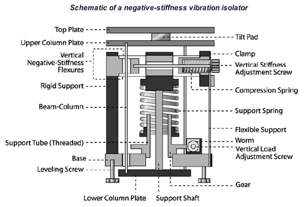
Vibration Isolation
STM requires extreme mechanical stability.
Even tiny vibrations can disturb measurements.
Special vibration isolation systems are used to maintain stability.
Working Mechanism of STM
The scanning tunneling microscope operates through several steps.
- A sharp conductive tip is brought extremely close to the sample surface.
- A voltage is applied between the tip and the surface.
- Electrons tunnel across the gap, creating a measurable current.
- The tip scans across the surface using piezoelectric actuators.
- Changes in tunneling current are recorded and converted into an image.
Because tunneling current depends on the distance between the tip and surface, STM images reveal atomic-scale surface features.
Imaging Modes of STM
STM can operate in different modes depending on how the tunneling current is controlled.
Constant Current Mode
In this mode:
- The tunneling current is kept constant.
- The feedback system adjusts the tip height.
The recorded tip motion produces a topographic image of the surface.
Constant Height Mode
In this mode:
- The tip height remains fixed.
- Variations in tunneling current are recorded.
This mode is faster but requires extremely flat surfaces.
Atomic Resolution Imaging

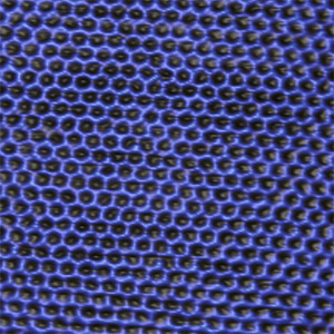


One of the most remarkable achievements of STM is its ability to resolve individual atoms.
Atomic-resolution images reveal:
- Atomic lattice structures
- Surface defects
- Adsorbed atoms and molecules
STM images have confirmed theoretical predictions about atomic arrangements on crystal surfaces.
Spectroscopy with STM
STM can also perform scanning tunneling spectroscopy (STS).
STS measures how tunneling current changes with applied voltage.
This allows scientists to study:
- Electronic states of materials
- Local density of states
- Surface electronic properties
STS provides important information about semiconductor surfaces and nanomaterials.
Atomic Manipulation

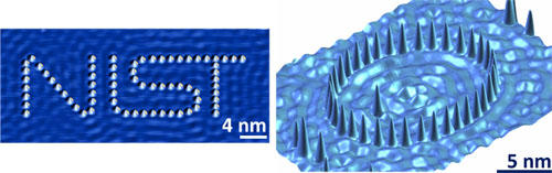


One of the most famous demonstrations of STM was the manipulation of individual atoms.
Researchers at IBM arranged xenon atoms to spell “IBM”.
Using STM tips, scientists can:
- Move individual atoms
- Build nanoscale structures
- Study atomic interactions
This capability has opened new possibilities in nanotechnology.
Applications of Scanning Tunneling Microscopy
STM has many scientific and technological applications.
Surface Science
STM is widely used to study atomic arrangements on material surfaces.
Researchers investigate:
- Surface defects
- Atomic diffusion
- Surface reactions
Nanotechnology
STM enables manipulation and assembly of nanoscale structures.
This is important for developing nanodevices and quantum materials.
Semiconductor Research
STM is used to study electronic properties of semiconductor surfaces.
It helps improve microelectronics and chip manufacturing.
Catalysis Research
STM allows scientists to observe catalytic reactions occurring on surfaces.
This improves understanding of industrial catalysts.
Materials Science
STM helps analyze crystal structures, thin films, and nanomaterials.
Researchers study defects, grain boundaries, and electronic properties.
Advantages of STM
Scanning tunneling microscopy offers several advantages.
Atomic Resolution
STM can image individual atoms.
Surface Sensitivity
STM provides detailed information about surface structures.
Electronic Information
STM reveals electronic properties of materials.
Atomic Manipulation
Atoms can be moved and positioned with high precision.
Limitations of STM
Despite its advantages, STM has some limitations.
Conductive Samples Required
STM generally works only with conductive or semiconductive materials.
Environmental Sensitivity
STM requires stable environments free from vibration and noise.
Slow Imaging
Scanning can be relatively slow compared with other imaging techniques.
STM in Modern Research
Modern STM techniques include advanced capabilities such as:
- Low-temperature STM
- Ultra-high vacuum STM
- Spin-polarized STM
- Time-resolved STM
These developments allow researchers to study quantum phenomena and atomic-scale processes in unprecedented detail.
STM vs Other Microscopy Techniques
STM is often compared with other nanoscale imaging techniques.
Compared to optical microscopy:
- STM provides much higher resolution.
Compared to electron microscopy:
- STM images surfaces directly at atomic scale.
Compared to atomic force microscopy:
- STM measures tunneling current rather than mechanical force.
Each technique has unique advantages depending on the application.
Future of STM
STM continues to evolve with improvements in:
- Nanotechnology
- Quantum materials research
- Atomic-scale electronics
- Surface chemistry
Future STM systems may enable precise construction of atomic-scale devices.
These advances could contribute to the development of quantum computers and nanoscale electronic systems.
Conclusion
Scanning tunneling microscopy is one of the most powerful tools for studying surfaces at the atomic level. By exploiting the quantum tunneling effect, STM can measure extremely small distances and produce images of individual atoms.
Since its invention, STM has transformed nanotechnology and materials science by enabling researchers to observe and manipulate atoms directly. Applications range from semiconductor research and surface chemistry to atomic-scale engineering.
As technology advances, STM continues to expand the boundaries of scientific exploration, providing deeper insight into the atomic structure of matter and enabling the development of new nanoscale technologies.